IBM Just Broke the 1nm Barrier. It Still Can't Make the Chip.
IBM has unveiled 'nanostack,' the world's first sub-1nm (0.7nm) chip research. Some say it adds a decade to Moore's Law; others say a lab demo is a long way from a fab. Either way, mass production isn't IBM's job.
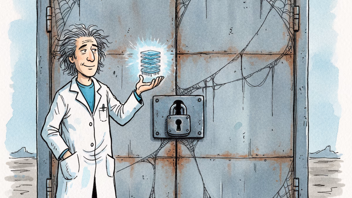
One fingernail-sized chip, 100 billion transistors. That's the headline number from the sub-1nm (below one nanometer) chip research IBM revealed on June 25, 2026. The company called it a world first. That's accurate — but it comes with an asterisk. It's a world first in the *research lab*, and there's no factory yet lined up to actually build the thing.
At an event in the US, IBM Research announced a new transistor architecture called “nanostack,” aimed at a 0.7nm (7-angstrom) node. The findings were presented at the VLSI 2026 semiconductor conference (IBM Newsroom, June 25). The industry split into two camps almost immediately. One side said the work “adds 10 to 15 years to the Moore's Law roadmap.” The other drew a hard line: a breakthrough on a lab bench and a chip rolling off a production line are two very different things.
First, let's unpack that “0.7nm” number
Here's something that trips up a lot of readers: since the 7nm generation, chip node names haven't measured anything physical. They're closer to marketing labels than rulers. IBM's “0.7nm” is no exception — if you actually measured the transistor, you wouldn't find anything that size. The nanosheet layers are reportedly around 5nm thick (Slashdot community commentary, for reference). You'll often see “0.7nm equals the width of an atom” tossed around, but that's an analogy, not a measurement.
So what did IBM actually pull off? It changed direction. Until now, shrinking chips has been a 2D game: drawing the components smaller and smaller on a flat plane. But transistors have run into quantum interference limits, and that flat approach is hitting a wall (MIT Technology Review, June 25). Nanostack's answer is to build upward — stacking nanosheet transistors vertically and offsetting them, a 3D approach. IBM says it combined wafer bonding, SRAM scaling, and new channel materials to get there.
By the numbers: IBM says transistor density roughly doubles versus its 2021 2nm chip, with performance up as much as 50% and energy efficiency up as much as 70%. SRAM cells shrank 40%. All told, a fingernail-sized chip lands at roughly 100 billion transistors (IBM Newsroom).
Some secondary outlets reported that, used as an AI accelerator, the chip could deliver around 7,000 TOPS and slash AI model training times. But that figure cites an IBM estimate and isn't confirmed in the official press release. It's too early to treat it as a hard number.
The optimists: a decade added to Moore's Law
The case from the cheering section is straightforward. If shrinking really is hitting a wall, then stacking upward is a fresh way forward.
Industry analyst Dan Hutcheson characterized the technology as adding “10 to 15 years to the roadmap” (MIT Technology Review). IBM itself says the nanostack roadmap supports at least another decade of scaling.
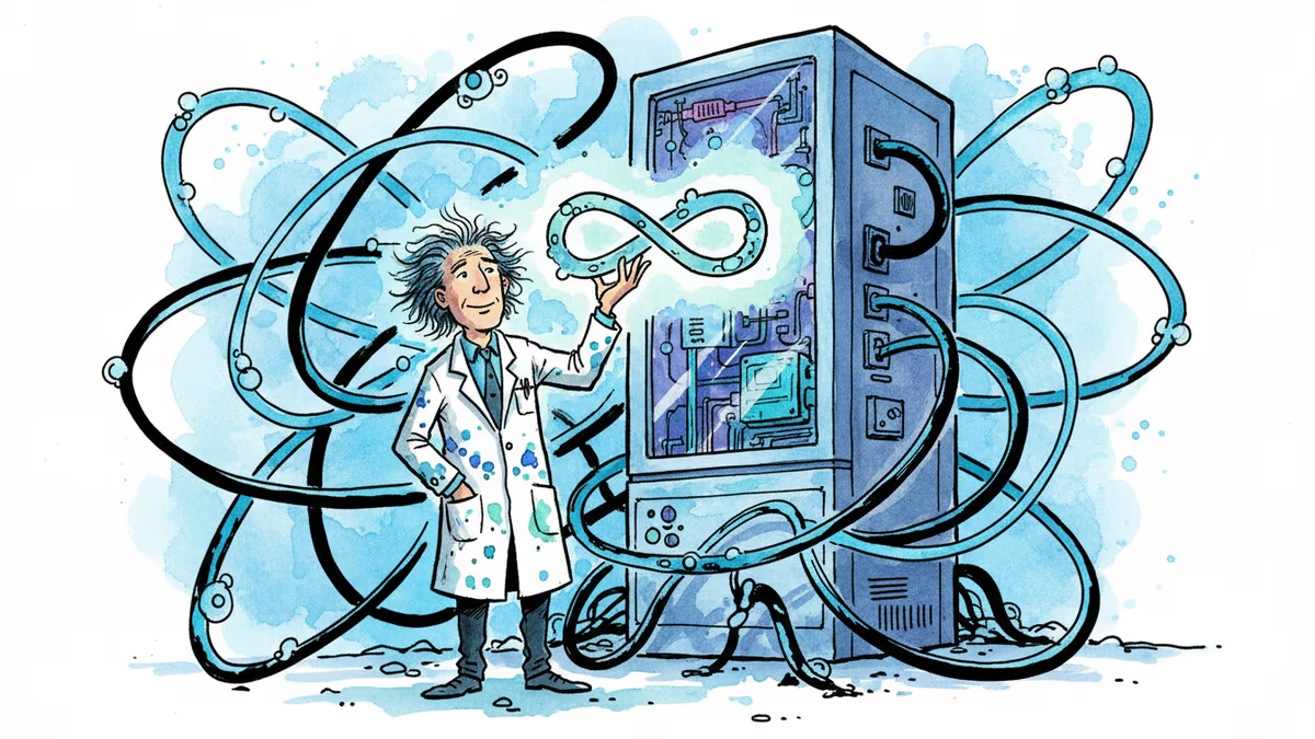
Here's the part worth pausing on: this foundational architecture didn't come out of Silicon Valley or an Asian foundry. It came out of an American research lab. Jay Gambetta, director of IBM Research, said the point of nanostack isn't just to make smaller transistors — it's to reinvent how chips are made in the first place (IBM Newsroom). Whatever happens in the race to mass-produce, the blueprint for the next generation of chips was drawn in a US lab. For a country that has spent years watching leading-edge manufacturing drift to Taiwan and South Korea, that's a notable data point in the R&D column.
The skeptics: a lab result and a fab are different leagues
The other side is calm about it. Their point is simple: inventing something and mass-producing it are two different problems.
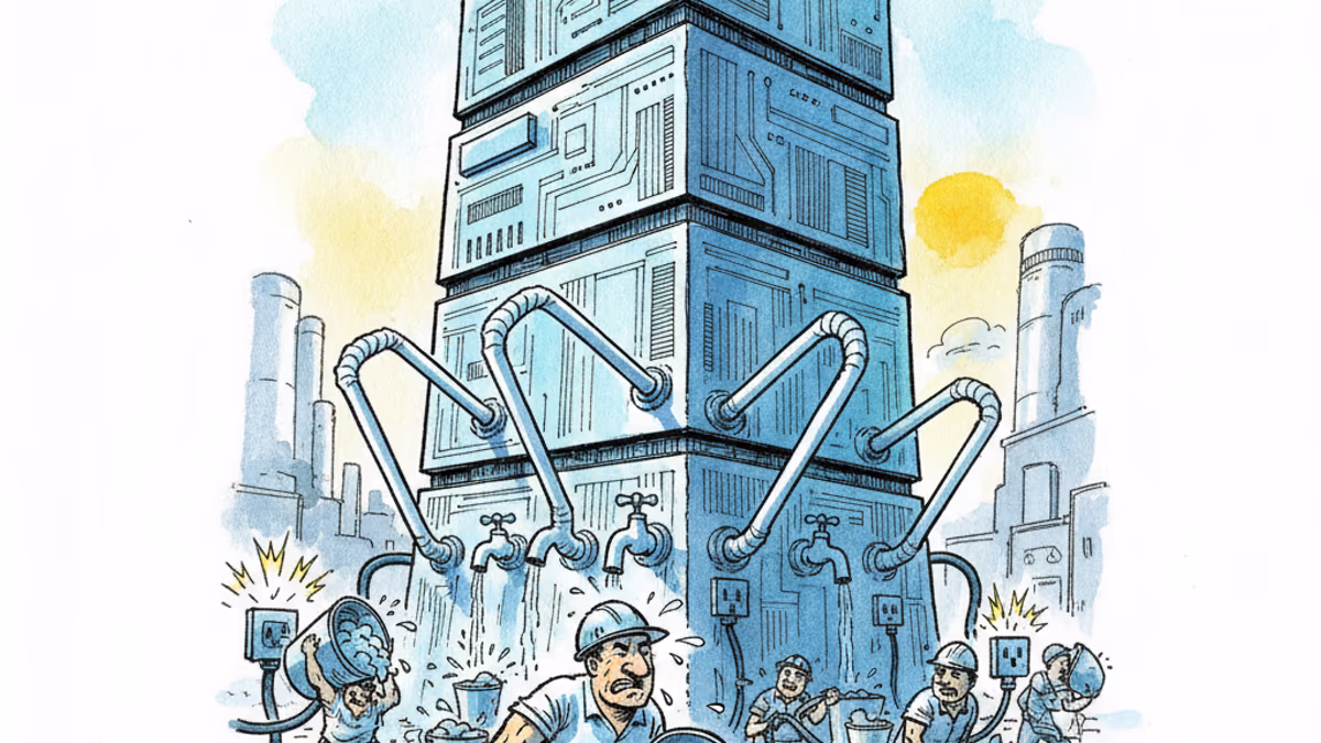
First, yield. Stack components on top of each other and the defect rate climbs. As MIT Technology Review noted, if any single layer in the stack fails, the whole chip fails. The more layers, the more the odds of a defect multiply.
Second, heat. 3D stacking concentrates heat in a tight space. The process has to stay below 400°C (752°F), and IBM hasn't disclosed exactly how it solved that (MIT Technology Review).
Third, timing. IBM's stated target for early partner production is within five years — roughly 2031. In other words, this is a “five years out, if all goes well” technology. On community forums, some dismissed it as an announcement timed to prop up the quarterly stock price (Slashdot, for reference).
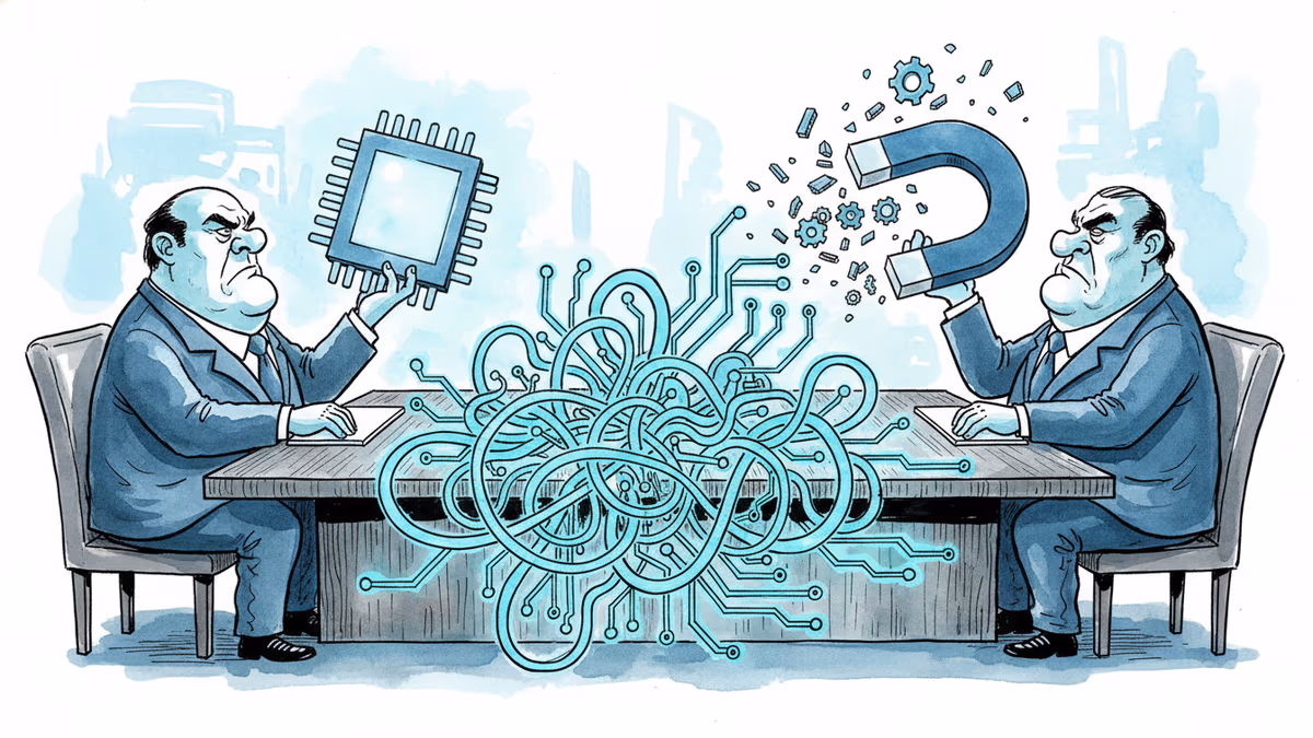
And here's the crux. IBM isn't a foundry. This is the piece global readers most often miss: IBM Research invents architectures, but outside partners actually manufacture the chips. In the past that role fell to GlobalFoundries; today it's foundries like Samsung and Rapidus. For this 0.7nm work, no manufacturing partner has been named yet. So “IBM is making a 1nm chip” isn't quite right. Think of IBM less like Intel or TSMC — which design *and* build — and more like Arm or a university lab: it hands the design to someone else to fabricate.
What “world first” actually weighs
Some context helps. Taiwan's TSMC has already started 2nm mass production (TechNews, UDN). Most of today's AI chips are 5nm and 4nm class, and TSMC makes the bulk of them.
So these two milestones are different in kind. TSMC's 2nm is a *production* milestone — running in a fab right now. IBM's 0.7nm is a *research* milestone, aimed five years out. Both matter, but you can't weigh them on the same scale. IBM's “world first” is a first for sub-1nm research demonstration, not a first for mass production.
The real contest isn't about size
IBM doesn't sell this chip. IBM Research invents the architecture; foundries like Samsung, TSMC, and Rapidus do the actual manufacturing. So the real battleground for “0.7nm” isn't transistor size — it's who can turn this 3D stacking into a mass-production yield. There's a precedent worth remembering: in 2021, IBM's foundational 2nm technology ended up not at Samsung but at Rapidus, a Japanese startup foundry. That's a reminder that source technology and manufacturing capability are separate leagues. Which fab this 0.7nm work lands in will decide its real industrial impact.
What to watch: not the node name, but “how many layers”
The number to watch here may not be “0.7nm” at all. It's the nanostack 3D-stacking paradigm itself.
The roadmap nanostack lays out assumes early partner production around 2031. While TSMC is already mass-producing 2nm, IBM's 0.7nm still has a manufacturing problem to solve: how many layers can you stack reliably? As node names drift further from physical dimensions, controlling yield and heat becomes the deciding variable for whether any of this can actually be built at scale.
So the next round of news comes down to two questions: which foundry IBM partners with, and whether that partner can handle 3D stacking at yield. Gambetta's blueprint is on the table. Now it's the factory's turn to answer.
This content is AI-generated based on source articles. While we strive for accuracy, errors may occur. We recommend verifying with the original source.
Related Articles
Samsung and SK unveiled a chip and AI investment package worth thousands of trillions of won on June 29. The headline number swings wildly by outlet, but the real contest isn't capital — it's water and power.
As Trump and Xi meet in Beijing, five tech flashpoints—chips, AI rivalry, supply chains, EVs, and rare earths—will quietly shape the global economy more than any diplomatic communiqué.

Consumer SSD prices have surged up to 400% since late 2025. WD, Samsung, SanDisk all affected. We unpack the NAND supply crunch, tariff effects, and what comes next.
IBM's quantum computer contributed to synthesizing a half-Möbius topology molecule. What this experiment reveals about quantum computing's slow march toward real-world utility.
Samsung and SK unveiled a chip and AI investment package worth thousands of trillions of won on June 29. The headline number swings wildly by outlet, but the real contest isn't capital — it's water and power.
As Trump and Xi meet in Beijing, five tech flashpoints—chips, AI rivalry, supply chains, EVs, and rare earths—will quietly shape the global economy more than any diplomatic communiqué.
Consumer SSD prices have surged up to 400% since late 2025. WD, Samsung, SanDisk all affected. We unpack the NAND supply crunch, tariff effects, and what comes next.
IBM's quantum computer contributed to synthesizing a half-Möbius topology molecule. What this experiment reveals about quantum computing's slow march toward real-world utility.
Thoughts
Share your thoughts on this article
Sign in to join the conversation